The Dual-Port RAM Modules
-
DPRAM Repo, BoxLambda fork, boxlambda branch: https://github.com/epsilon537/verilog-wishbone.
-
DPRAM Submodule in the BoxLambda Directory Tree: boxlambda/sub/verilog_wishbone/.
-
DPRAM Component in the BoxLambda Directory Tree: boxlambda/gw/components/wb_dp_ram
-
DPRAM Core Top-Level: gw/components/wb_dp_ram/rtl/wb_dp_ram_wrapper.sv
-
XPM_MEMORY_TDPRAM Documentation: https://docs.xilinx.com/r/en-US/ug974-vivado-ultrascale-libraries/XPM_MEMORY_TDPRAM
The wb_dpram_wrapper.sv module selects one of two DPRAM implementations depending on whether we're targeting simulation or FPGA synthesis.
On FPGA, I'm using an XPM_MEMORY_TDPRAM instance. Using an XPM macro for internal memory allows me to do post-synthesis memory image updates in the bitstream file, as described here.
I did run into a spurious write issue with XPM_MEMORY_TDPRAM. To avoid the issue, I had to qualify the Write Enable (wea/web) signals with the valid signals even though the valid signals were already going to the module's Memory Enable ports (ena/enb):
    assign a_valid    = a_cyc_i & a_stb_i;
    assign b_valid    = b_cyc_i & b_stb_i;
    ...
    assign a_ram_we   = {4{a_we_i&a_valid}} & a_sel_i;
    assign b_ram_we   = {4{b_we_i&b_valid}} & b_sel_i;
    ...
    .ena(a_valid),                       // 1-bit input: Memory enable signal for port A. Must be high on clock
                                        // cycles when read or write operations are initiated. Pipelined
                                        // internally.

    .enb(b_valid),                       // 1-bit input: Memory enable signal for port B. Must be high on clock
                                        // cycles when read or write operations are initiated. Pipelined
                                        // internally.
    ...
    .wea(a_ram_we),                     // WRITE_DATA_WIDTH_A/BYTE_WRITE_WIDTH_A-bit input: Write enable vector
                                        // for port A input data port dina. 1 bit wide when word-wide writes are
                                        // used. In byte-wide write configurations, each bit controls the
                                        // writing one byte of dina to address addra. For example, to
                                        // synchronously write only bits [15-8] of dina when WRITE_DATA_WIDTH_A
                                        // is 32, wea would be 4'b0010.

    .web(b_ram_we)                      // WRITE_DATA_WIDTH_B/BYTE_WRITE_WIDTH_B-bit input: Write enable vector
                                        // for port B input data port dinb. 1 bit wide when word-wide writes are
                                        // used. In byte-wide write configurations, each bit controls the
                                        // writing one byte of dinb to address addrb. For example, to
                                        // synchronously write only bits [15-8] of dinb when WRITE_DATA_WIDTH_B
                                        // is 32, web would be 4'b0010.
    ...
In simulation, I'm using Alex Forencich's wb_dp_ram.v module.
Two Dual Port RAMs
BoxLambda's internal memory consists of two Dual Port instances: CMEM and DMEM. The two instances create a Harvard Architecture (see below). The RAMs are Dual Port to allow simultaneous memory access from both the CPU and the DMA Controller.
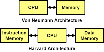
Harvard vs. Von Neumann Architecture.
In a Von Neumann Architecture, the CPU has access to one memory that stores both instructions and data. Instruction Fetch and Data Access transactions share one memory bus. In a Harvard Architecture, Instruction Memory is separate from Data Memory. Instruction Fetch and Data Access transactions can be executed independently.
The Ibex processor has separate Instruction and Data ports. When accessing internal memory, the instruction port by default targets CMEM, and the data port by default targets DMEM. These defaults can be overridden by mapping data to the .cmem_bss section and code to the .dmem_text section. See the Link Script section for details.
DPRAM Clock Frequency
The two DPRAM instances, CMEM and DMEM, are part of the 50MHz System Clock Domain.