Components
We're building a System-on-a-Chip (System-on-an-FPGA?). This section identifies the Key Components of the BoxLambda SoC.
The Bus
The Bus, or interconnect, is the fabric stitching together the SoC internal components. For this project, the two most relevant SoC internal bus specifications are ARM's AXI bus and the Open-Source Wishbone bus.
AXI is very powerful, very popular, and very complex. It scales up well to very big SoCs. However, I don't think it scales down very well to simple SoCs, such as BoxLambda, where low latency and low complexity are more important than high bandwidth and scalability. Hence, for this project, I'm electing to go with Wishbone.
We'll be using the Wishbone B4 specification.
Sticking to a well-defined internal bus specification certainly helps to meet the Modular Architecture Requirement. Whether we can also accommodate Partial FPGA Reconfiguration using a Wishbone Interconnect remains to be seen.
The Processor
Processor Word Size
Typical processor word sizes are 8-bit, 16-bit, 32-bit, and 64-bit. Which word size is the best fit for Boxlambda?
- 8-bit: A good word size.
- Pros:
- An 8-bit word (i.e. a byte) is a good natural fit for a pixel value, an ASCII character code, or small integer values.
- 8-bit processors, their programs, and their data are very compact.
- 8-bit processors side-step some of the alignment issues seen with larger word sizes.
- Cons:
- An 8-bit word is too small to conveniently hold the values you need in a typical program - think calculations and table indices.
- Toolchain support for higher-level languages is limited.
- 16-bit: A clumsy compromise between 8-bit and 32-bits. Made sense when 32-bit processors were not readily available yet. Now, not so much.
- 32-bit: Another good word size.
- Pros: 32-bit words can hold most real-world numbers and cover a huge address space. 32-bit machines generally have good toolchain support.
- Cons: Much bigger than its 8-bit counterpart, in terms of FPGA real estate, program size as well as data size.
- 64-bit: A big and clunky word size, way too big to handle conveniently, intended for specialized use cases that don't fit this project.
I've decided to go for a 32-bit processor. A 32-bit processor (and associated on-chip memory) will take a bigger chunk out of our FPGA real estate, but I think it's worth it. I like the convenience of 32-bit registers, and a 32-bit processor may come with a regular GCC toolchain.
Processor Features
Next to a 32-bit word size, we're looking for the following features for our microprocessor:
- Ease of programming, meaning:
- Easy and well-documented Instruction Set Architectures (ISA). We want to be able to program the machine at assembly language level.
- Shallow Pipeline: It is relatively easy to reason about the behavior of a processor with a two-stage pipeline. It is not very easy to reason about the behavior of a processor with a six-stage pipeline.
- Good toolchain support, such as GCC, so we can build a software ecosystem for our machine.
- An accessible and well-documented implementation.
- Has to fit our FPGA, with enough space to fit the other components.
With all that in mind, I think RISC-V is a great option.
- Great ISA, building on lessons learned from previous popular processor architectures.
- 32-bit support.
- GCC toolchain support.
- Open-Source.
- Well-documented.
- Very fashionable. Let's ride that wave :-)
The CPU core: Ibex
There are a lot of RISC-V implementations to choose from. The Ibex project seems like a good choice:
https://github.com/lowRISC/ibex
- 32-bit RISC-V.
- High-quality, well-documented implementation.
- SystemVerilog based. My preferred HDL.
- Supports a small two-stage pipeline parameterization.
- Very active project.
Location of the Ibex submodule in the BoxLambda repo: sub/ibex/
The Ibex core: sub/ibex/rtl/ibex_top.sv
The Wishbone Wrapper: Ibex_WB
https://github.com/epsilon537/ibex_wb forked from https://github.com/batuhanates/ibex_wb
The Ibex RISCV core itself doesn't have Wishbone ports. Ibex_WB wraps around the vanilla Ibex core and attaches Wishbone port adapters to its instruction and data ports.
The Ibex_WB repo also includes an example SoC build consisting of an Ibex core connected via a shared Wishbone bus to a wbuart32 core and an internal memory module, along with the software to run on that platform. This example SoC is the starting point for BoxLambda's implementation. See the Test Builds section below.
Location of the Ibex_WB submodule in the BoxLambda repo: sub/ibex/
The wb_ibex_core: sub/ibex_wb/rtl/wb_ibex_core.sv
Ibex Core Configuration
I settled on RISCV configuration RV32IMCB: The (I)nteger and (C)ompressed instruction set are fixed in Ibex. (M)ultiplication and Division and (B)it Manipulation are enabled optional extensions. Note that there's no Instruction or Data Cache. Code executes directly from DPRAM or DDR memory. Data access also goes straight to DPRAM or DDR memory. The Ibex core is instantiated with the following M and B parameters, as shown in the Ibex_wb ibex_soc example:
sub/ibex_wb/soc/fpga/arty-a7-35/rtl/ibex_soc.sv:
wb_ibex_core #(
  .RV32M(ibex_pkg::RV32MFast),
  .RV32B(ibex_pkg::RV32BBalanced),
  ...
  ) wb_ibex_core (
  ...
  .boot_addr    (32'h0),
  ...
Wb_ibex_core's boot_addr port is a misnomer. Boot_addr specifies the base address of the vector table. The Reset Vector, i.e. the first instruction executed when the processor comes out of reset, is at offset 0x80 relative to this base address. Hence, the real Boot Address for BoxLambda is address 0x80.
The Debug Unit: RISCV-DBG
https://github.com/epsilon537/riscv-dbg forked from https://github.com/pulp-platform/riscv-dbg.
RISCV OpenOCD
OpenOCD is an open-source software package used to interface with a hardware debugger's JTAG port via one of many transport protocols. In our case, the hardware debug logic is implemented by a component called riscv-dbg. The overall setup looks like this:
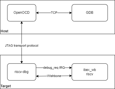
OpenOCD General Setup
BoxLambda uses the RISCV fork of OpenOCD: https://github.com/riscv/riscv-openocd
The RISCV-DBG component
RISCV-dbg is part of the PULP platform and depends on three additional GitHub repositories that are part of this platform: - common_cells: https://github.com/pulp-platform/common_cells - tech_cells_generic: https://github.com/pulp-platform/tech_cells_generic - pulpino: https://github.com/pulp-platform/pulpino
As their names suggest, common_cells and tech_cells_generic provide commonly used building blocks such as FIFOs, CDC logic, reset logic, etc. Pulpino is an entire RISCV-based SoC project. However, the riscv-dbg pulpino dependency is limited to just a few cells for clock management.
I created git submodules for all of these repositories under the BoxLambda repository's sub/ directory. I then created a riscv-dbg component directory with a Bender.yml manifest in it, referencing all the sources needed from those submodules: components/riscv-dbg/Bender.yml.
boxlambda
├── components
│   └── riscv-dbg
│       └── Bender.yml
└── sub
    ├── common_cells
    ├── tech_cells_generic
    ├── pulpino
    └── riscv-dbg
RISCV-DBG RTL Structure
RISCV-DBG has two top-levels: - sub/riscv-dbg/src/dm_top.sv - sub/riscv-dbg/src/dmi_jtag.sv
Recall that BoxLambda uses a Wishbone interconnect. The Ibex_WB submodule implements a Wishbone wrapper for the Ibex RISCV core. It does the same for RISCV-DBG's dm_top:
sub/ibex_wb/rtl/wb_dm_top.sv
Refer to the ibex_soc example to see how RISCV-DBG is instantiated:
sub/ibex_wb/soc/fpga/arty-a7-35/rtl/ibex_soc.sv
OpenOCD and RISCV-DBG on Verilator
The JTAG transport protocol used on the Verilator Model is a simple socket-based protocol called Remote Bitbang. The remote bitbang spec is just one page:
https://github.com/openocd-org/openocd/blob/master/doc/manual/jtag/drivers/remote_bitbang.txt
The Verilator setup looks like this:

BoxLambda OpenOCD Verilator Setup
The hello_dbg project (directory projects/hello_dbg/) implements the OpenOCD Verilator setup shown above. The project contains the Hello World test build extended with the riscv-dbg component. The project directory also contains a test script that goes through the following steps: 1. Start the Verilator model 2. Connect OpenOCD to the model 3. Connect GDB to OpenOCD (and thus to the model) 4. Execute a UART register dump on the target 5. Check the UART register contents against expected results.
boxlambda
├── projects
│   └── hello-dbg
│       ├── Bender.yml
│       ├── sim
│       │   ├── sim_main.cpp
│       │   └── sim_main.sv
│       └── test
│           ├── test.sh
│           └── test.gdb
├── components
│   └── riscv-dbg
└── sub
    ├── common_cells
    ├── tech_cells_generic
    ├── pulpino
    └── riscv-dbg
The OpenOCD configuration file for JTAG Debugging on Verilator is checked into the openocd directory:
openocd/verilator_riscv_dbg.cfg
To summarize:
- The above OpenOCD config file is used to connect to the JTAG TAP of a Verilator model.
- The JTAG TAP is implemented by a riscv-dbg core connected to an Ibex RISCV32 core.
- The JTAG TAP is used to debug the software running on the Ibex RISCV32 core.
- The JTAG TAP is accessed using a socket-based OpenOCD transport protocol called remote_bitbang.
See the Test Builds section below for the steps needed to set up an OpenOCD JTAG debug session on Verilator.
OpenOCD and RISCV-DBG on Arty-A7 FPGA
The obvious approach would be to bring out the JTAG signals to PMOD pins and hook up a JTAG adapter. However, there's an alternative method that doesn't require a JTAG adapter. The riscv-dbg JTAG TAP can be hooked into the FPGA scan chain which is normally used to program the bitstream into the FPGA. On the Arty-A7, bitstream programming is done using the FTDI USB serial port, so no special adapters are needed.
The riscv-dbg codebase lets you easily switch between a variant with external JTAG pins and a variant that hooks into the FPGA scan chain, by changing a single file: - dmi_jtag_tap.sv: hooks up the JTAG TAP to external pins - dmi_bscane_tap.sv: hooks the JTAG TAP into the FPGA scan chain. The Xilinx primitive used to hook into the scan chain do this is called BSCANE. Hence the name.
Both files implement the same module name (dmi_jtag_tap) and the same module ports, so you can swap one for the other without further impact on the system. Lightweight polymorphism.
On the OpenOCD side, the transport protocol for this Debug-Access-via-FPGA-scan-chain-over-FTDI is anti-climactically called ftdi.

BoxLambda OpenOCD Arty A7 FTDI Setup
The OpenOCD configuration file for JTAG Debugging on Arty A7 is checked into the openocd directory:
openocd/digilent_arty_a7.cfg
To summarize:
- The above OpenOCD config file is used to connect to the JTAG TAP of a riscv-dbg core...
- ...to debug the software running on a connected Ibex RISCV32 core.
- The riscv-dbg core's JTAG TAP is hooked into the Arty-A7's scan chain, normally used for loading a bitstream into the FPGA.
- The Arty-A7 FPGA scan chain is accessible through the board's FTDI-based USB serial port.
- The OpenOCD transport protocol name for this type of connection is ftdi.
See the Test Builds section below for the steps needed to set up an OpenOCD JTAG debug session on the Arty A7.
The Memory Controller
SDRAM memory access is pretty complicated. Memory access requests get queued in the memory controller, scheduled, and turned into a sequence of commands that vary in execution time depending on the previous memory locations that were recently accessed.
There exists a class of memory controllers, called Static Memory Controllers, that absorb these complexities and by design create a fixed schedule for a fixed use case, resulting in very predictable behavior. Static Memory Controllers are far off the beaten path, however. Dynamic Memory Controllers are more common. Dynamic Memory Controllers can handle a variety of use cases with good performance on average. Unfortunately, they sacrifice predictability to achieve this flexibility.
Ideally, we would use an accessible, well-documented, open-source, static memory controller design. Unfortunately, I can't find one. Rolling our own is not an option either. Doing so would require so much specific know-how, that it would kill this project. Pragmatically, our best option is to use Xilinx's Memory Interface Generator (MIG) with the Arty A7 (or Nexys A7) parameters as published by Diligent.
The Xilinx memory controller falls squarely into the Dynamic Memory Controller class. How do we fit this into a platform that requires deterministic behavior? I think the best approach is to use a DMA engine to transfer data between SDRAM and on-chip memory. Fixed memory access latency to on-chip memory (from any bus master that requires it) can be guaranteed using an arbiter. We'll revisit this topic when we're discussing Boxlambda's architecture.
The Graphics Subsystem
If you're reading this, you must be into the build-your-own-computer thing, which probably means you're aware of the super cool Commander X16 project. Frank van de Hoef created the very elegant VERA (Video Embedded Retro Adapter) module for the X16. Here's a high-level specification, taken from the Commander X16 website:
VERA module specifications:
- Video generator featuring:
- Multiple output formats (VGA, NTSC Composite, NTSC S-Video, RGB video) at a fixed resolution of 640x480@60Hz
- Support for 2 layers, both supporting:
- 1/2/4/8 bpp tile and bitmap modes
- Support for up to 128 sprites (with inter-sprite collision detection).
- Embedded video RAM of 128 KB.
- Palette with 256 colors selected from a total range of 4096 colors.
- 16-channel stereo Programmable Sound Generator with multiple waveforms (Pulse, Sawtooth, Triangle, Noise)
- High-quality PCM audio playback from a 4 KB FIFO buffer featuring up to 48kHz 16-bit stereo sound.
- SecureDigital storage.
Other features, not mentioned in the blurb, include:
- Fractional display scaling (scaling lower resolutions up to the 640x480 display resolution).
- Horizontal and Vertical smooth scrolling
Lucky for us, Frank recently released the VERA Verilog code under the generous MIT license. You can find the code here:
https://github.com/fvdhoef/vera-module
I'm not particularly interested in VERA's PSG (Programmable Sound Generator), or the non-VGA output formats, so I might remove those from the build.
The 128KB of video RAM will take a big chunk out of our available Block RAM resources, but it'll be worth it. We're getting a lot of bang for our buck.
Note that the VERA is designed as a separate FPGA with a SPI slave interface. Some modifications will be required to integrate it into our SoC.
Sound
A sound core is a perfect candidate for Partial FPGA Reconfiguration. There are a lot of options (Wave-Table synthesis, FM synthesis, PSG...) and a lot of open-source cores available. It would be pretty cool if the software application can just download its synthesizer of choice as part of the program.
Pretty much any core developed by Jotego sounds like a great idea.
Technically, I don't have to select a sound core. We already have sound through VERA's PCM audio playback. I'm going to select a sound core anyway because I like retro sounds and I'd like to mess around a bit with one of the old-school PSG chips.
I think I'll go for a dual YM2149, one for music, one for sound FX, in a game context. The YM2149 was the Atari ST's sound chip, so we'll have a large music and sound FX archive at our disposal. Jotego developed an FPGA clone of the YM2149, the JT49:
https://github.com/jotego/jt49
DMA
I was on the fence for a while, deciding whether or not I should include a DMA engine in our machine. In a previous post, I said I would use DMA to move data between external and internal memory. However, a DMA Controller is by definition a bus master, and having multiple bus masters (DMAC and CPU) adds significant complexity to the architecture: access to shared buses and slaves, impact on timing, etc. In a system with only one bus master, the CPU, you don't have to worry about any of that.
Then I snapped out of it and remembered that BoxLambda is intended to be a platform for RTL experimentation. It would be silly to restrict these RTL experiments to bus slave components only. In other words, the BoxLambda architecture is going to have to accommodate bus masters, so we might as well include a DMA Controller.
Some use cases for DMA in the scope of our computer include:
- Moving data between external (DDR) and internal (Block RAM) memory.
- Streaming from memory to the audio DAC.
- Blitting, i.e. copying data into video memory, taking into account the video memory's organization. For instance, copying a rectangular block of data into a frame buffer requires striding between rows of pixel data. Another example: Bit planes with 1, 2, or 4 bits-per-pixel color depths require barrel shifting when copying data to a specific pixel offset.
I spent many hours online searching for DMA Controllers. I was a bit surprised that there were so few options, so I kept digging. I found ZipCPU's, FreeCore's, and Ant Micro's DMA controllers. The Anti Micro DMAC seemed to be the most interesting option, with two Wishbone ports, pipelined mode, striding support, and support for any byte boundary alignment.
I was ready to go with the Ant Micro selection when I happened across an old post on Reddit where somebody proposed a 'smart' DMA concept: a DMAC with a tiny CPU embedded in it. That sounded like a great concept, so I pinged the author to check what became of his idea. In response, the author generously decided to release his code on GitHub! The core is called Praxos. Here is the repository:
https://github.com/esherriff/Praxos
Praxos has a tiny CPU with a small amount of program and data memory embedded in the core, allowing you to write microcode specifying the DMA behavior you want: word/non-word alignment, incrementing/decrementing/non-incrementing source and/or destination address, strides between transfers, combining sources, barrel shifting... Maximum flexibility!
It's not perfect though. Praxos only has one bus master port, an Avalon port at that. It should be doable to slap a standard Wishbone port onto it, but in its current form, I think it won't be able to take advantage of Wishbone's pipelined burst mode. That's unfortunate for a DMAC.
Still, having the option to hack together my own application-specific DMA microcode sounds like a lot of fun. I just have to go with the Praxos option.
Many thanks to esherriff for making his code available!
Storage
I'm going to use ZipCPU's SD Card Controller in combination with the FatFs software library to mount a FAT filesystem on the SD card:
- SD Card Controller: https://github.com/ZipCPU/sdspi
- FatFs library: http://elm-chan.org/fsw/ff/00index_e.html
The SD Card Controller has a Wishbone slave port.
Keyboard and Mouse
FreeCores has PS/2 keyboard and mouse modules: https://github.com/freecores/ps2
These cores don't have a Wishbone slave port, so we're going to have to add that ourselves.
Note that the Nexys A7 has a USB HID host interface for keyboard and mouse which, with the help of clever firmware on a PIC24 microcontroller, presents itself to the FPGA as a PS/2 interface. See the Nexys A7 Reference Manual for more details.
I2C
The I2C interface can be used to hook up a Real-Time Clock PMOD as well as a Wii Nunchuck Adapter.
ZipCPU has an I2C core with a Wishbone port: https://github.com/ZipCPU/wbi2c.
Serial Port
ZipCPU comes to the rescue once again with a UART implementation with a Wishbone interface: https://github.com/ZipCPU/wbuart32
Location of the wbuart32 submodule in the BoxLambda repository: boxlambda/fpga/wbuart32/
Miscellaneous Modules
- DFX Controller: The actual loading of a Reconfigurable Module into a Reconfigurable Partition is handled by the DFX Controller. DFX stands for Dynamic Function Exchange which is Xilinx-speak for Partial FPGA Reconfiguration.
- ICAP: Internal Configuration Access Port. This module gives access to the FPGA configuration functionality built into Xilinx FPGAs. We'll use the ICAP to implement in-system updates of the Full Configuration Bitstream, loaded into the FPGA upon boot-up.
- Quad SPI Flash: This is a module provided by Xilinx, giving access to the Flash Memory device attached through a Quad-SPI bus. The non-volatile Flash Memory will hold the Full Configuration Bitstream(s), System Firmware, and non-volatile system configuration parameters such as keyboard type
- wb_gpio: A simple GPIO core with a Wishbone interface, for sampling buttons and switches, and driving LEDs. wb_gpio.v is included in the Ibex_WB submodule.